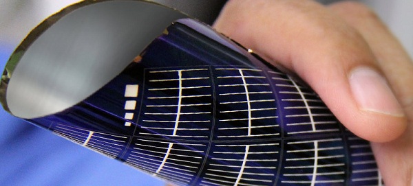
Skinnier might not always be better—You saw Angelina Jolie at the Oscars, right?—but when it comes to silicon wafers, the key building block in crystalline solar panels, thin is definitely in. And that’s why a new technology busted out today by the California company Twin Creeks Technologies could be a game-changer.
Twin Creeks unveiled a process that it says allows it to generate monocrystalline wafers that are less than a tenth the thickness of conventional wafers. The company said that by dramatically reducing the amount of silicon and other substrate materials used, its technology could lower the price of solar modules to 40 cents per watt—around half the current cost.

“The thickness of wafers today is based on wafer slicing capabilities and the handling requirements for device processing. In reality, only the very top layer of a substrate plays an active role in generating energy or transmitting signals—the rest is wasted,” Siva Sivaram, CEO of Twin Creeks, said in a statement. “By eliminating excess material, we will help solar manufacturers produce modules that compete with grid power and open up new markets for chip makers.”
Twin Creeks said the key to the process is a technique called proton induced exfoliation (PIE), in which a uniform layer of high-energy protons—hydrogen ions—are embedded into monocrystalline wafers to a depth of up to 20 microns. “When heated, this new layer expands, cleaving the top surface from the donor wafer to form an ultra-thin wafer that is otherwise identical to the original,” the company said. “The ultra-thin wafer is then further processed into solar modules or semiconductors.”

The common method for creating the wafers is to cut up silicon ingots, which produces 200-nanometer-thick slices and a great deal of kerf, or wasted silicon. Twin Creeks said its Hyperion system makes wafers that are 20 nanometers thick and with none of the kerf.
The focus on waste-reducing wafer processes isn’t peculiar to Twin Creeks; last fall we told you about 1366 Technologies, a Massachusetts company that says its own process reduces four separate manufacturing steps into a single, low cost continuous process and greatly reduces silicon waste by forming individual wafers directly from a bath of molten silicon. The company won a $150 million loan guarantee from the U.S. Department of Energy.
While 1366 is working to move from first generation to commercialization, Twin Creeks said Hyperion 3, the company’s first commercial offering, is available for shipment now. The company has what it calls a “commercial demonstration plant” in Senatobia, Miss., that it says is “currently capable of producing 25 megawatts of solar cells a year and will be expanded to 100 megawatts.”